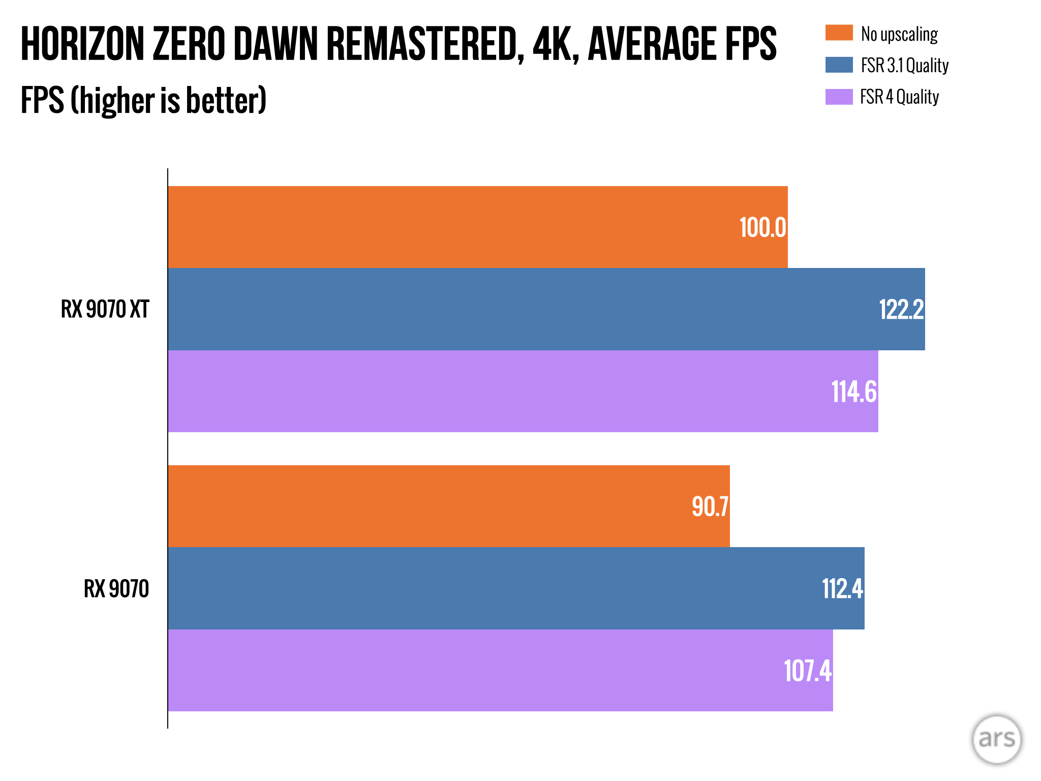
Framework “temporarily pausing” some laptop sales because of new tariffs
Framework, the designers and sellers of the modular and repairable Framework Laptop 13 and other products, announced today that it would be “temporarily pausing US sales” on some of its laptop configurations as a result of new tariffs put on Taiwanese imports by the Trump administration. The affected models will be removed from Framework’s online store for now, and there’s no word on when buyers can expect them to come back.
“We priced our laptops when tariffs on imports from Taiwan were 0 percent,” the company responded to a post asking why it was pausing sales. “At a 10 percent tariff, we would have to sell the lowest-end SKUs at a loss.”
“Other consumer goods makers have performed the same calculations and taken the same actions, though most have not been open about it,” Framework said. Nintendo also paused US preorders for its upcoming Switch 2 console last week after the tariffs were announced.
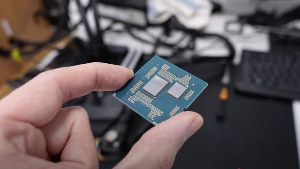
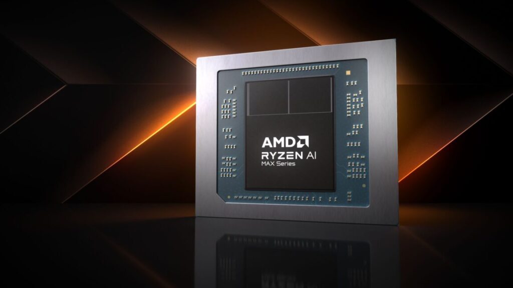
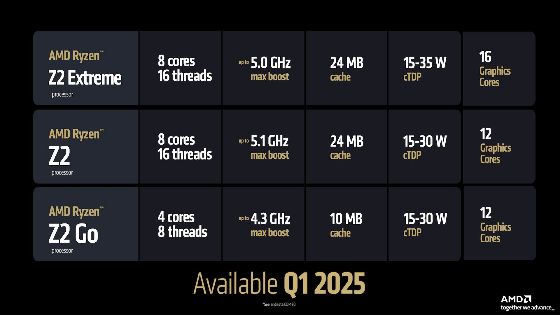
For right now, Framework’s sales pause affects at least two specific laptop configurations: the Intel Core Ultra 5 125H and AMD Ryzen 5 7640U versions of the Framework Laptop 13. As of April 1, Framework was selling pre-built versions of those laptops for $999 and $899, respectively. Without those options, the cheapest versions of those laptops start at $1,399 and $1,499.
Framework “temporarily pausing” some laptop sales because of new tariffs Read More »