chips and science act

micron’s-$6b-chips-funding-should-have-more-strings-attached,-critics-say

Micron’s $6B CHIPS funding should have more strings attached, critics say


Micron’s NY fabs are the only CHIPS projects undergoing full environmental review.

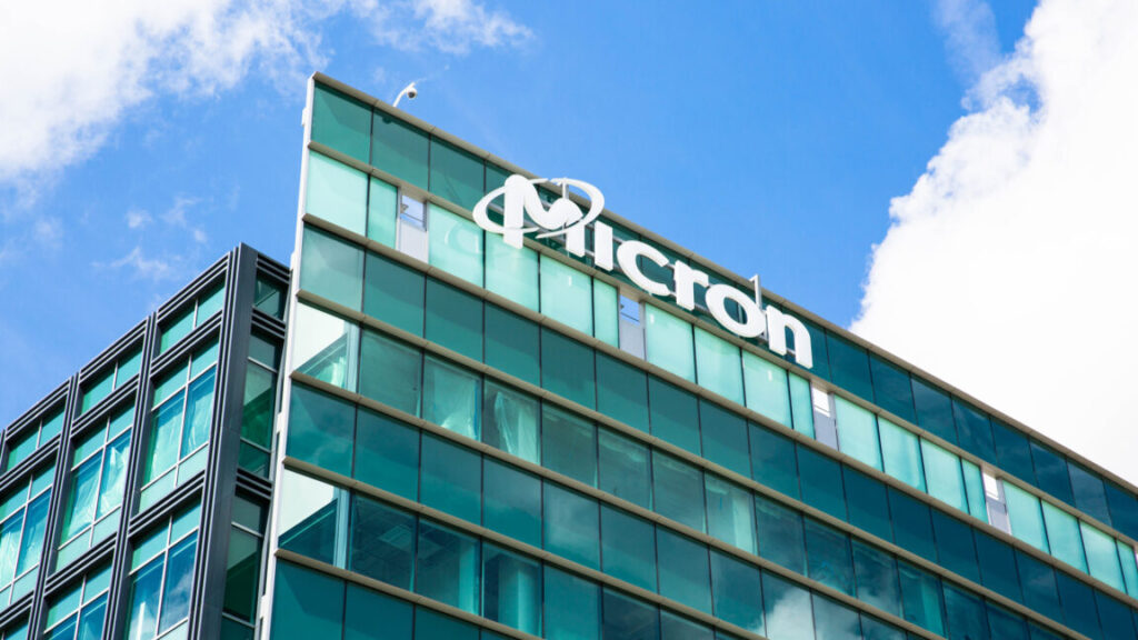
Micron Technology will receive more than $6.1 billion after the US Department of Commerce finalized one of the largest CHIPS Act awards ever to “the only US-based manufacturer of memory chips,” Vice President Kamala Harris said in a press statement.

Micron will use the funding to construct “several state-of-the-art memory chips facilities” in New York and Idaho, Harris said. The chipmaker has committed to a “$125 billion investment over the next few decades” and promised to create “at least 20,000 jobs,” Harris confirmed.

Additionally, Micron “agreed to preliminary terms for an additional investment of $275 million to expand” its facility in Manassas, Virginia, Harris confirmed. Those facilities will mostly be used to manufacture chips for automotive and defense industries, Harris noted.

Because of billions in CHIPS funding doled out by the Biden administration, Harris said, the US’s “share of advanced memory manufacturing” will go “from nearly 0 percent today to 10 percent over the next decade.”

The Semiconductor Industry Association, a trade and lobbying group that bills itself as “the voice of the semiconductor industry,” celebrated Micron’s award. In a press release, its president and CEO, John Neuffer, said that the award sets the US on a path to become a leading memory chip innovator.

“Memory is a technology critical to America’s economic future and national security, and Micron’s historic investments in producing memory chips in the US will strengthen US leadership for the long term,” Neuffer said.

In a statement, Micron President and CEO Sanjay Mehrotra said that “Micron is uniquely positioned to bring leading-edge memory manufacturing to the U.S., strengthening the country’s technology leadership and fostering advanced innovation.”

“Micron’s investments in domestic semiconductor manufacturing capabilities, supported by the bipartisan CHIPS Act, will help drive economic growth and ensure that the US remains at the forefront of technological advancements,” Mehrotra said.

Advocates: Micron needs to explain what a “good job” is

But while Neuffer joined Harris’ and the Commerce Department’s chorus, praising the award for creating “high-paying American jobs,” bolstering US national and economic security, and fueling “innovation for years to come,” communities are raising questions.

Advocates with Jobs to Move America (JMA)—who are organizing ahead of Micron’s New York construction starting in 2026—are concerned that Micron hasn’t been clear about what a “good job” is before moving into an area with “one of the highest poverty rates in the country.”

“There has been little discussion or firm commitments made regarding what exactly a ‘good job’ is, or how equitable access for said jobs will be achieved for current local residents,” JMA’s “Good Jobs Platform,” drafted earlier this year with more than 20 local advocacy groups, said.

“We define a ‘good job’ as one that guarantees: workers have a fair and clear process to organize a union without employer opposition, family-sustaining wages and comprehensive benefits, safe working conditions, equitable hiring and employment practices, and is supported by an accessible workforce pipeline,” the platform said.

And equally important are communities’ and workers’ health and safety concerns, the platform noted, urging that “a good job is a safe job.”

A senior researcher and policy coordinator for JMA, Anna Smith, told Ars that Harris’ statement was missing any mention of a community impact statement. And while Harris mentioned “utilizing project labor agreements and registered apprenticeship programs, which will further strengthen local economies” and “support workers,” more enforceable commitments are needed to protect communities as Micron’s construction begins, Smith said.

The “Good Jobs Platform” recommends a range of commitments, from labor peace agreements that would ensure workers can unionize to community workforce agreements keeping workers involved in key discussions regarding ongoing training and career development. Local labor leaders have sought similar commitments, urging Micron to commit to a community benefits agreement “that enshrines legally enforceable provisions that protect the community, its workers, and the environment.”

In his statement, Mehrotra said that Micron had formed local partnerships to build a “community investment framework” that would “revitalize central New York.”

Micron first CHIPS fabs to get full environmental review

More transparency is also urgently needed regarding Micron’s environmental commitments, advocates told Ars. In New York, Micron’s fabs are preparing to wipe out over 200 acres of mature forested wetlands, and so far, Micron has not provided a public “detailed mitigation plan to compensate for the loss,” a local environmental expert, Catherine Landis, warned during a public comment period on Micron’s plan to pave over the wetlands.

Unlike any other fab site in the US receiving CHIPS Act funding, Micron’s New York fabs must release a full environmental impact statement (EIS), which is currently being drafted and expected to be distributed to agencies this month, advocates told Ars. Construction has been delayed until the EIS is completed, at which point the public will gain a better understanding of how much harm could be caused by the project and what steps Micron will take to mitigate harms.

JMA has warned about potential impacts, like increased flooding in the area impacting both communities and Micron’s fabs. Destroying the wetlands will also displace federally protected endangered animal populations, JMA said, including the northern long-eared bat and the sedge wren. Potential chemical spills, reported at other US fabs, could endanger water quality, as could any mismanaged handling of chemical waste. And perhaps most critically, the energy demand to operate Micron’s facilities could risk setting back New York’s climate goals, JMA advocates said.

More transparency would help communities better prepare to welcome Micron and other chipmakers developing fabs across the US. JMA and local experts have agreed that the promised economic benefits Micron’s fabs will deliver in New York are a positive development, as are Micron’s commitments guaranteeing New York construction workers can unionize.

But communities will likely be the ones raising alarms as Micron’s operations introduce to the environment “thousands of compounds used in chip manufacture (most unregulated)” with “short- and long-term effects on plants, animals, people” still largely unknown, Landis said. And that’s where JMA hopes to make an impact, submitting freedom of information acts to request undisclosed data and pushing for community benefit agreements and other commitments from Micron to ensure communities aren’t irreversibly harmed by new fabs.

JMA expects that the EIS could help galvanize communities preparing for Micron’s construction to start in New York.

“I do think it is a really helpful tool that we have in our belt, and something that will help the public engage about concerns that we have,” Smith told Ars. “It spans, of course, air emissions, wastewater, runoff, toxics, wetlands, but it also includes things like housing and transportation, and those are things that we think that the Syracuse community is very concerned about.”

The EIS could mean that New York residents have a clearer understanding of how CHIPS funding may be polluting their communities. Most of the other communities nationwide impacted by CHIPS projects likely won’t have the same level of detailed information. Eric Romann, a JMA regional director, told Ars that, while “it’s positive that a higher bar has been set” for Micron’s New York project, that’s only “compared to the very low bar set for the other projects around the country, or you could say very low to non-existent bar.”

Micron declined to comment directly on workers’ concerns. In a statement provided to Ars, Micron’s spokesperson said that “Micron is committed to environmental stewardship across our global operations, including developing and maintaining critical environmental protections for our planned investment” in New York.

“A required environmental impact statement is currently in production with both federal and state lead agencies, and we are working closely with government stakeholders to ensure we meet any environmental permitting required for the project,” Micron’s spokesperson said. “We look forward to engaging with the public and government stakeholders during comment periods for the project’s draft environmental impact statement and environmental permitting in the near future.”

Photo of Ashley Belanger

Ashley is a senior policy reporter for Ars Technica, dedicated to tracking social impacts of emerging policies and new technologies. She is a Chicago-based journalist with 20 years of experience.

Micron’s $6B CHIPS funding should have more strings attached, critics say Read More »
biden-rushes-to-avert-labor-shortage-with-chips-act-funding-for-workers

Biden rushes to avert labor shortage with CHIPS act funding for workers

Less than one month to apply —

To dodge labor shortage, US finally aims CHIPS Act funding at training workers.

US President Joe Biden (C) speaks during a tour of the TSMC Semiconductor Manufacturing Facility in Phoenix, Arizona, on December 6, 2022.

Enlarge / US President Joe Biden (C) speaks during a tour of the TSMC Semiconductor Manufacturing Facility in Phoenix, Arizona, on December 6, 2022.

In the hopes of dodging a significant projected worker shortage in the next few years, the Biden administration will finally start funding workforce development projects to support America’s ambitions to become the world’s leading chipmaker through historic CHIPS and Science Act investments.

The Workforce Partner Alliance (WFPA) will be established through the CHIPS Act’s first round of funding focused on workers, officials confirmed in a press release. The program is designed to “focus on closing workforce and skills gaps in the US for researchers, engineers, and technicians across semiconductor design, manufacturing, and production,” a program requirements page said.

Bloomberg reported that the US risks a technician shortage reaching 90,000 by 2030. This differs slightly from Natcast’s forecast, which found that out of “238,000 jobs the industry is projected to create by 2030,” the semiconductor industry “will be unable to fill more than 67,000.”

Whatever the industry demand will actually be, with a projected tens of thousands of jobs needing to be filled just as the country is hoping to produce more chips than ever, the Biden administration is hoping to quickly train enough workers to fill openings for “researchers, engineers, and technicians across semiconductor design, manufacturing, and production,” a WFPA site said.

To do this, a “wide range of workforce solution providers” are encouraged to submit “high-impact” WFPA project proposals that can be completed within two years, with total budgets of between $500,000 and $2 million per award, the press release said.

Examples of “evidence-based workforce development strategies and methodologies that may be considered for this program” include registered apprenticeship and pre-apprenticeship programs, colleges or universities offering semiconductor industry-relevant degrees, programs combining on-the-job training with effective education or mentorship, and “experiential learning opportunities such as co-ops, externships, internships, or capstone projects.” While programs supporting construction activities will not be considered, programs designed to “reduce barriers” to entry in the semiconductor industry can use funding to support workers’ training, such as for providing childcare or transportation for workers.

“Making investments in the US semiconductor workforce is an opportunity to serve underserved communities, to connect individuals to good-paying sustainable jobs across the country, and to develop a robust workforce ecosystem that supports an industry essential to the national and economic security of the US,” Natcast said.

Between four to 10 projects will be selected, providing opportunities for “established programs with a track record of success seeking to scale,” as well as for newer programs “that meet a previously unaddressed need, opportunity, or theory of change” to be launched or substantially expanded.

The deadline to apply for funding is July 26, which gives applicants less than one month to get their proposals together. Applicants must have a presence in the US but can include for-profit organizations, accredited education institutions, training programs, state and local government agencies, and nonprofit organizations, Natcast’s eligibility requirements said.

Natcast—the nonprofit entity created to operate the National Semiconductor Technology Center Consortium—will manage the WFPA. An FAQ will be provided soon, Natcast said, but in the meantime, the agency is giving a brief window to submit questions about the program. Curious applicants can send questions to [email protected] until 11: 59 pm ET on July 9.

Awardees will be notified by early fall, Natcast said.

Planning the future of US chip workforce

In Natcast’s press release, Deirdre Hanford, Natcast’s CEO, said that the WFPA will “accelerate progress in the US semiconductor industry by tackling its most critical challenges, including the need for a highly skilled workforce that can meet the evolving demands of the industry.”

And the senior manager of Natcast’s workforce development programs, Michael Barnes, said that the WFPA will be critical to accelerating the industry’s growth in the US.

“It is imperative that we develop a domestic semiconductor workforce ecosystem that can support the industry’s anticipated growth and strengthen American national security, economic prosperity, and global competitiveness,” Barnes said.

Biden rushes to avert labor shortage with CHIPS act funding for workers Read More »

us-funds-$5b-chip-effort-after-lagging-on-semiconductor-innovation

US funds $5B chip effort after lagging on semiconductor innovation

Now hiring? —

US had failed to fund the “science half” of CHIPS and Science Act, critic said.

US President Joe Biden speaks before signing the CHIPS and Science Act of 2022.

Enlarge / US President Joe Biden speaks before signing the CHIPS and Science Act of 2022.

The Biden administration announced investments Friday totaling more than $5 billion in semiconductor research and development intended to re-establish the US as a global leader manufacturing the “next generation of semiconductor technologies.”

Through sizeable investments, the US will “advance US leadership in semiconductor R&D, cut down on the time and cost of commercializing new technologies, bolster US national security, and connect and support workers in securing good semiconductor jobs,” a White House press release said.

Currently, the US produces “less than 10 percent” of the global chips supply and “none of the most advanced chips,” the White House said. But investing in programs like the National Semiconductor Technology Center (NSTC)—considered the “centerpiece” of the CHIPS and Science Act’s four R&D programs—and training a talented workforce could significantly increase US production of semiconductors that the Biden administration described as the “backbone of the modern economy.”

The White House projected that the NSTC’s workforce activities would launch in the summer of 2024. The Center’s prime directive will be developing new semiconductor technologies by “supporting design, prototyping, and piloting and through ensuring innovators have access to critical capabilities.”

Moving forward, the NSTC will operate as a public-private consortium, involving both government and private sector institutions, the White House confirmed. It will be run by a recently established nonprofit called the National Center for the Advancement of Semiconductor Technology (Natcast), which will coordinate with the secretaries of Commerce, Defense, and Energy, as well as the National Science Foundation’s director. Any additional stakeholders can provide input on the NSTC’s goals by joining the NSTC Community of Interest at no cost.

The National Institute of Standards and Technology (NIST) has explained why achieving the NSTC’s mission to develop cutting-edge semiconductor technology in the US will not be easy:

The smallest dimensions of leading-edge semiconductor devices have reached the atomic scale and the complexity of the circuit architecture is increasing exponentially with the use of three-dimensional structures, the incorporation of new materials, and improvements in the thousands of process steps needed to make advanced chips. Into the future, as new applications demand higher-performance semiconductors, their design and production will become even more complex. This complexity makes it increasingly difficult and costly to implement innovations because of the dependencies between design and manufacturing, between manufacturing steps, and between front-end and back-end processes.

The complexity of keeping up with semiconductor tech is why it’s critical for the US to create clear pathways for skilled workers to break into this burgeoning industry. The Biden administration said it plans to invest “at least hundreds of millions of dollars in the NSTC’s workforce efforts,” creating a Workforce Center of Excellence with locations throughout the US and piloting new training programs, including initiatives engaging underserved communities. The Workforce Center will start by surveying best practices in semiconductor education programs, then establish a baseline program to attract workers seeking dependable paths to break into the industry.

Last year, the Semiconductor Industry Association (SIA) released a study showing that the US was not adequately preparing a highly skilled workforce. Between “67,000, or 58 percent, of projected new jobs, may remain unfulfilled at the current trajectory,” SIA estimated.

A skilled workforce is just part of the equation, though. The US also needs facilities where workers can experiment with new technologies without breaking the bank. To that end, the Department of Commerce announced it would be investing “at least $200 million” in a first-of-its-kind CHIPS Manufacturing USA Institute. That institute will “allow innovators to replicate and experiment with physical manufacturing processes at low cost.”

Other Commerce Department investments announced include “up to $300 million” for advanced packaging R&D necessary for discovering new applications for semiconductor technologies and over $100 million in funding for dozens of projects to help inventors “more easily scale innovations into commercial products.”

A Commerce Department spokesperson told Ars that “the location of the NSTC headquarters has not yet been determined” but will “directly support the NSTC research strategy and give engineers, academics, researchers, engineers at startups, small and large companies, and workforce developers the capabilities they need to innovate.” In 2024, NSTC’s efforts to kick off research appear modest, with the center expecting to prioritize engaging community members and stakeholders, launching workforce programs, and identifying early start research programs.

So far, Biden’s efforts to ramp up semiconductor manufacturing in the US have not gone smoothly. Earlier this year, TSMC predicted further delays at chips plants under construction in Arizona and confirmed that the second plant would not be able to manufacture the most advanced chips, as previously expected.

That news followed criticism from private entities last year. In November, Nvidia CEO Jensen Huang predicted that the US was “somewhere between a decade and two decades away” from semiconductor supply chain independence. The US Chamber of Commerce said last August that the reason why the US remained so far behind was because the US had so far failed to prioritize funding in the “science half” of the CHIPS and Science Act.

In 2024, the Biden administration appears to be attempting to finally start funding a promised $11 billion total in research and development efforts. Once NSTC kicks off research, the pressure will be on to chase the Center’s highest ambition of turning the US into a consistent birthplace of life-changing semiconductor technologies once again.

US funds $5B chip effort after lagging on semiconductor innovation Read More »